Driving the Evolution of Next-Generation Computing with Cutting-Edge Semiconductor Design & Verification
As next-generation computing, including AI, continues to evolve, semiconductor design and verification play a crucial role in accelerating this transformation. Our expertise extends to major applications such as AI servers, HPC, and autonomous driving, where we take charge of critical verification processes. By deeply understanding our clients' challenges and delivering tailored, optimal solutions, we have built strong, lasting relationships based on trust and excellence.
Work-Life Balance
We are committed to fostering an environment where engineers can unleash their full creative potential. Since our founding, we have prioritized a workplace culture that encourages productivity and innovation. With a flat organizational structure, we cultivate an open and collaborative atmosphere where ideas flow freely and technical knowledge is shared naturally.
Our remote-first policy minimizes commuting burdens and enables flexible work arrangements, empowering engineers to achieve both professional and personal fulfillment. Additionally, our comprehensive support system ensures that everyone can take advantage of paid leave, parental leave, and caregiving leave with ease and confidence.
Join us and take your career to new heights while crafting the ideal work-life balance you've been looking for.
As cutting-edge technologies like AI find applications in areas such as autonomous driving, the importance of design and verification technologies for achieving highly integrated SoCs has never been greater. Meanwhile, the rise of innovative approaches like chiplets is driving increased specialization in semiconductor development, with each domain focusing on its core expertise. As a result, improving the quality of individual components has become a more critical challenge than ever before. Leveraging our extensive experience and proven track record in verification, we are committed to supporting our customers in bringing competitive, high-quality products to market swiftly and efficiently.
Our vision is to become the leading provider of innovative SoC verification(and design) solutions, driving the future of semiconductor technology and nurturing the highest quality design and verification engineers through excellence in engineering a commitment to customer success, while at the same time developing high-quality design and verification engineers who are the foundation of the semiconductor industry.
Our mission is to deliver comprehensive, high-quality RTL design and verification services that enable clients to develop cutting-edge technologies efficiently and reliably. We strive to achieve this through continuous innovation, strategic partnerships, and a dedicated focus on customer satisfaction and technical excellence.
| Comapany Name | Verifore Inc. | |
|---|---|---|
| Establishment Date | September 20, 2007 | |
| Representative Director | Arnold Foster Jensen | |
| Director | Dallin Kay Barton | |
| Director | Jingyan Wei | |
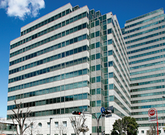
| Head Office | YBP West Tower 7F, 134 Godo-cho, Hodogaya-ku, Yokohama, Kanagawa 240-0005 Japan | |
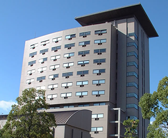
| Technology Center | Keihanna Plaza Laboratory Wing, 1-7, Hikaridai, Seika-cho, Souraku-gun, Kyoto, 619-0237 Japan | |
| URL | https://www.verifore.jp/ | |
| info@verifore.jp |
A 4-minute walk from Sotetsu Line " Tennocho Station "
A 7-minute walk from Sotetsu Line "Hoshikawa Station" (South Exit)
For more details, please refer to the official website below:
Yokohama Business Park Official
A 10-minute taxi ride from Kintetsu Keihanna Line "Gakken Nara Tomigaoka Station"
A 10-minute taxi ride from JR "Hosono Station"
A 10-minite taxi ride from Kintetsu Kyoto Line "Shin-Hosono Station"
For more details, please refer to the official website below: